OEM Optics for the Semiconductor Industry. Resolve the Finest Structures.
The trend of smaller and smaller structures on semiconductor chips continues. For purposes of inspection, optical instruments in the DUV range (< 300 nm) are used today.
With our modern production facility in Heerbrugg, we are able to meet the increasing requirements of the semiconductor industry.
We operate cleanrooms of class ISO 5 (100) with very clean work zones under flow boxes. Special to manufacturing and assembly processes for 193 nm optics, we have high-quality cleanrooms with VOC (volatile organic compounds) controlled air, filtering out the VOC parts to below 2 ng/l (nanograms per liter).
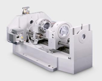
Customer-specific modules to inspect reticles and wafers
A majority of reticles produced, that are used to illuminate wafers, have been inspected by the high-resolution and precise optics from SwissOptic at least once in their lives.
Our contribution to your success
- Customer-specific designs (optical and mechanical) as well as cost-optimized production and assembly
- Specially designed measurement techniques to qualify complete modules
- Many years of experience in cleanroom assembly of opto-mechanical modules for the semiconductor industry
- Highly specialized employees

Optic modules for reticle inspection
For further specifications please refer to our technical data sheet
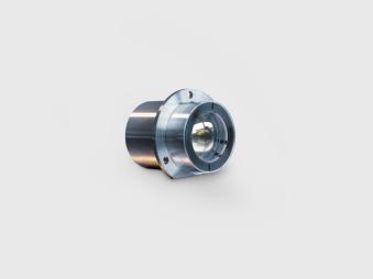
Customer-specific lenses for high-end applications
The lenses from SwissOptic provide an essential contribution to the high performance of measurement devices. To do so, they cover a wavelength range from 193 to 1,300 nm.
Our contribution to your success
- Customer-specific designs (optical and mechanical) as well as cost-optimized production and assembly
- Fully developed designs in mounting, centering and adjustment techniques to achieve a wavefront of the entire module of below λ 0.04 RMS (λ working wavelength)
- Many years of experience in cleanroom assembly of high-end lenses for the semiconductor industry
- Diffraction-limited lenses
- Specially designed measurement techniques to qualify complete lenses
- Highly specialized employees
- One-stop shop (design/manufacture/assembly and qualification)

Customer-specific DUV lens
For further specifications please refer to our technical data sheet
Special optical components for the semiconductor industry
At our Heerbrugg location, we have notably mastered the production of retardation plates in the DUV range with an accuracy of up to λ 1/100. Additional precise components in our portfolio include optically contacted beam splitters, optical tunnels for beam homogenization as well as complex, optically contacted mirror systems.
Our contribution to your success
- Specific design and production know-how
- Lenses and prisms with shape accuracies of under λ/100
- Beam splitters and mirrors
- Aspheres
- Microroughness of below 0.3 nm (3A)
- Coatings with a high destruction threshold (193 nm to IR)
- Broadband coatings
- Polarization optics
- Specially designed DUV measurement

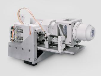
Customized modules for mask inspection
Contact our specialists
Please choose your contact partner:


